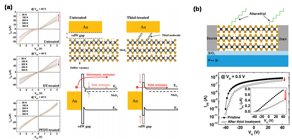
Ref. Kyungjune Cho et al., “Contact-Engineered Electrical Properties of MoS2 Field-Effect Transistors via Selectively Deposited Thiol-Molecules”, Advanced Materials, 30, 1705540 (2018)
Ref. Kyungjune Cho et al., "Electrical and optical characterization of MoS2 with sulfur vacancy passivation by treatment with alkanethiol molecules", ACS Nano, 9, 8044 (2015)
All 2D van der Waals (vdWs) heterostructures has been attracted much attention due to their unique properties such as gate tunability, new functionality compared with conventional devices. This vdWs heterostructures are not limited to 2D layered materials. 2D materials and organic polymers can also form vdWs heterostructures due to their dangling-bond free interface. We study 2D materials/organic polymers vdWs heterostructure system for
new functionality device.

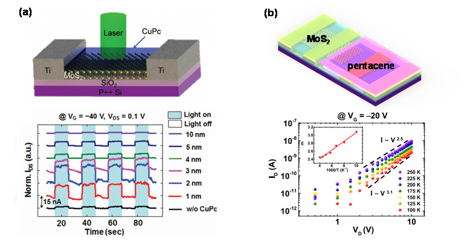
Ref. Jae-Keun Kim et al., "Trap-mediated electronic transport properties of gate-tunable pentacene/MoS2 p-n heterojunction diodes", Scientific Reports, 6, 36775 (2016)
Ref. Jinsu Pak et al. "Enhancement of Photodetection Characteristics of MoS2 Field Effect Transistors using Surface Treatment with Copper Phthalocyanine", Nanoscale, 7, 18780 (2015)
2.Optoelectronic device
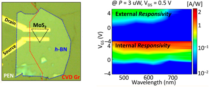
2D materials have been extensively studied as promising candidate for realizing flexible photodetector due to its outstanding optoelectronic properties, such as direct band gap of its monolayer, high carrier mobility, and mechanical flexibility.We study underlying physics of 2D materials based optoelectronic device for application as flexible photodetector.

Ref. Jinsu Pak et al., "Intrinsic Optoelectronic Characteristics ofMoS2 Phototransistors via a Fully Transparentvan der Waals Heterostructure", ACS Nano, 13, 9638 (2019)
3.MoS2 grown by chemical vapor deposition (CVD)
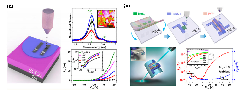
To utilize 2D materials in large area integrated application, it is desirable to grow uniform large area 2D materials. CVD method is one of promising candidate for uniform large area synthesis of 2D materials. We study CVD grown MoS2FET fabricated by ink jet printing method for large area application. Also, we study charge transport of CVD grown MoS2.
Ref. Tae-young Kim et al., "Transparent Large-Area MoS2 Phototransistors with Inkjet-Printed Components on Flexible Platforms", ACS Nano, 11, 10273 (2017)
Ref. Tae-Young Kim, Matin Amani, Geun Ho Ahn, Younggul Song, Ali Javey, Seungjun Chung, Takhee Lee, "Electrical Properties of Synthesized Large-Area MoS2 Field-Effect Transistors Fabricated with Inkjet-Printed Contacts", ACS Nano, 10, 2819 (2016)
